Техническая документация
Характеристики
Brand
Renesas ElectronicsТип продукции
Драйвер буфера/тактового сигнала
Тип монтажа
Поверхность
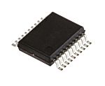
Корпус
SSOP
Минимальное напряжение питания
3V
Число контактов
20
Максимальная поддерживаемая емкость памяти
3.6V
Минимальная рабочая температура
-40°C
Максимальная рабочая температура
85°C
Стандарты/одобрения
Нет
Серия
49FCT
Автомобильный стандарт
Нет
Информация о товаре
The Renesas Electronics buffer/non-inverting clock driver built using advanced dual metal CMOS technology. The device consists of two banks of drivers, each with a 1:5 fanout and its own output enable control. The device has a heartbeat monitor for diagnostics and PLL driving. The MON output is identical to all other outputs and complies with the output specifications in this document. It offers low capacitance inputs with hysteresis. It is designed for high speed clock distribution where signal quality and skew are critical. It is also allows single point-topoint transmission line driving in applications such as address distribution, where one signal must be distributed to multiple recievers with low skew and high signal quality.
Информация о наличии не успела загрузиться
P.O.A.
Each (In a Pack of 5) (ex VAT)
Стандартная упаковка
5
P.O.A.
Each (In a Pack of 5) (ex VAT)
Информация о наличии не успела загрузиться
Стандартная упаковка
5
Техническая документация
Характеристики
Brand
Renesas ElectronicsТип продукции
Драйвер буфера/тактового сигнала
Тип монтажа
Поверхность
Корпус
SSOP
Минимальное напряжение питания
3V
Число контактов
20
Максимальная поддерживаемая емкость памяти
3.6V
Минимальная рабочая температура
-40°C
Максимальная рабочая температура
85°C
Стандарты/одобрения
Нет
Серия
49FCT
Автомобильный стандарт
Нет
Информация о товаре
The Renesas Electronics buffer/non-inverting clock driver built using advanced dual metal CMOS technology. The device consists of two banks of drivers, each with a 1:5 fanout and its own output enable control. The device has a heartbeat monitor for diagnostics and PLL driving. The MON output is identical to all other outputs and complies with the output specifications in this document. It offers low capacitance inputs with hysteresis. It is designed for high speed clock distribution where signal quality and skew are critical. It is also allows single point-topoint transmission line driving in applications such as address distribution, where one signal must be distributed to multiple recievers with low skew and high signal quality.